- 您现在的位置:买卖IC网 > Sheet目录484 > NDT454P (Fairchild Semiconductor)MOSFET P-CH 30V 5.9A SOT-223
Electrical Characteristics (T A = 25°C unless otherwise noted)
Symbol
Parameter
Conditions
Min
Typ
Max
Units
DRAIN-SOURCE DIODE CHARACTERISTICS AND MAXIMUM RATINGS
I S
Maximum Continuous Drain-Source Diode Forward Current
-1.9
A
V SD
Drain-Source Diode Forward Voltage
V GS = 0 V, I S = -5.9 A
(Note 2)
-0.85
-1.3
V
t rr
Reverse Recovery Time
V GS = 0V, I F = -5.9 A, dI F /dt = 100 A/μs
100
ns
Notes:
1. R θ JA is the sum of the junction-to-case and case-to-ambient thermal resistance where the case thermal reference is defined as the solder mounting surface of the drain pins. R θ JC is guaranteed by
design while R θ CA is determined by the user's board design.
P D ( t ) =
T J ? T A
R θ JA ( t )
=
T J ? T A
R θ JC + R θ CA ( t )
= I 2 D ( t ) × R DS ( ON )
T J
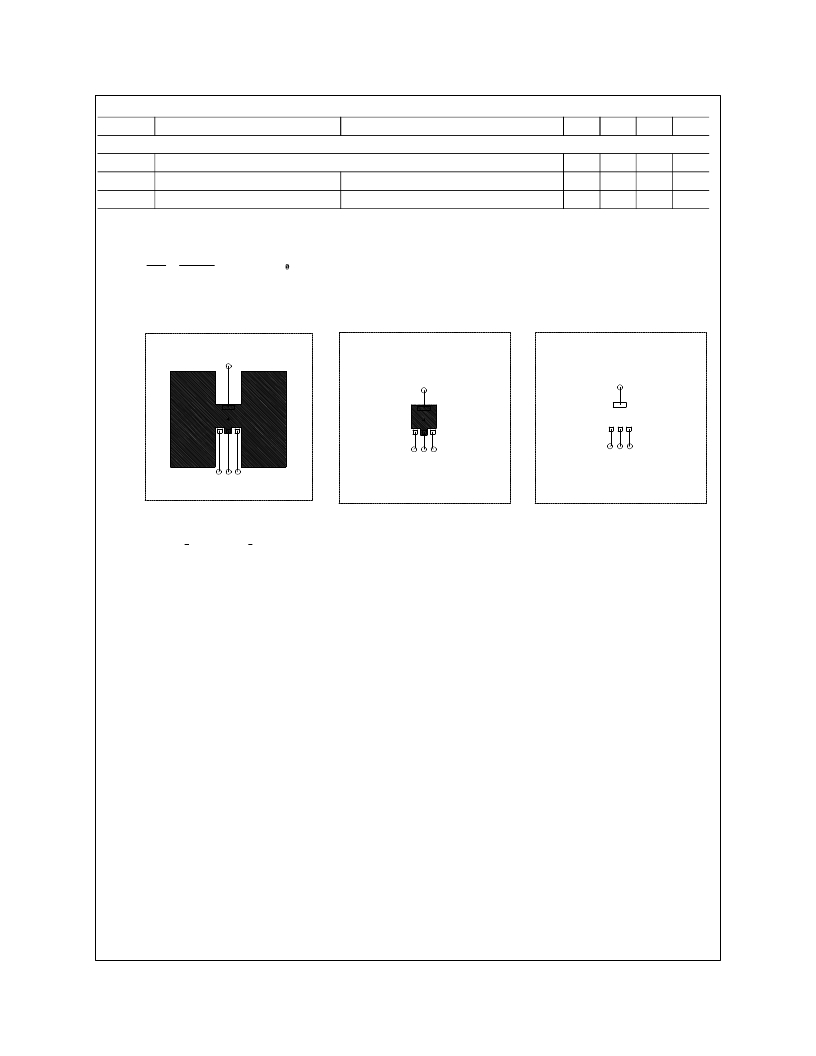
Typical R θ JA using the board layouts shown below on 4.5"x5" FR-4 PCB in a still air environment:
a. 42 o C/W when mounted on a 1 in 2 pad of 2oz copper.
b. 95 o C/W when mounted on a 0.066 in 2 pad of 2oz copper.
c. 110 o C/W when mounted on a 0.0123 in 2 pad of 2oz copper.
1a
1b
1c
Scale 1 : 1 on letter size paper
2. Pulse Test: Pulse Width < 300μs, Duty Cycle < 2.0%.
NDT454P Rev. D2
发布紧急采购,3分钟左右您将得到回复。
相关PDF资料
NDT456P
MOSFET P-CH 30V 7.5A SOT-223-4
NE34018-EVGA19
EVAL BOARD NE34018 1.9GHZ
NE5520279A-EVPW09
EVAL BOARD NE5520279A 900MHZ
NE6510179A-EVPW35
EVAL BOARD NE6510179A 3.5GHZ
NE651R479A-EVPW35
EVAL BOARD NE651R479A 3.5GHZ
NHD-COG14-36
ADAPTER SMT TO 2.54MM THRU-HOLE
NHD-TS-12864ARNB#
TOUCH PANEL 82X50.2MM 4-WIRE
NHD-TS-12864CRNA#
TOUCH PANEL 71.3X55MM 4-WIRE
相关代理商/技术参数
NDT454P(J23Z)
制造商:FAIRCHILD 制造商全称:Fairchild Semiconductor 功能描述:TRANSISTOR | MOSFET | P-CHANNEL | 30V V(BR)DSS | 5.9A I(D) | SOT-223
NDT454P
制造商:Fairchild Semiconductor Corporation 功能描述:TRANSISTOR
NDT455N
功能描述:MOSFET SOT-223 N-CH ENHANCE RoHS:否 制造商:STMicroelectronics 晶体管极性:N-Channel 汲极/源极击穿电压:650 V 闸/源击穿电压:25 V 漏极连续电流:130 A 电阻汲极/源极 RDS(导通):0.014 Ohms 配置:Single 最大工作温度: 安装风格:Through Hole 封装 / 箱体:Max247 封装:Tube
NDT455N(J23Z)
制造商:FAIRCHILD 制造商全称:Fairchild Semiconductor 功能描述:TRANSISTOR | MOSFET | N-CHANNEL | 30V V(BR)DSS | 11.5A I(D) | SOT-223
NDT456
制造商:FAIRCHILD 制造商全称:Fairchild Semiconductor 功能描述:P-Channel Enhancement Mode Field Effect Transistor
NDT456P
功能描述:MOSFET SOT-223 P-CH ENHANCE RoHS:否 制造商:STMicroelectronics 晶体管极性:N-Channel 汲极/源极击穿电压:650 V 闸/源击穿电压:25 V 漏极连续电流:130 A 电阻汲极/源极 RDS(导通):0.014 Ohms 配置:Single 最大工作温度: 安装风格:Through Hole 封装 / 箱体:Max247 封装:Tube
NDT456P(J23Z)
制造商:FAIRCHILD 制造商全称:Fairchild Semiconductor 功能描述:TRANSISTOR | MOSFET | P-CHANNEL | 30V V(BR)DSS | 7.5A I(D) | SOT-223
NDT456P
制造商:Fairchild Semiconductor Corporation 功能描述:MOSFET P LOGIC SOT-223
